back to homepage
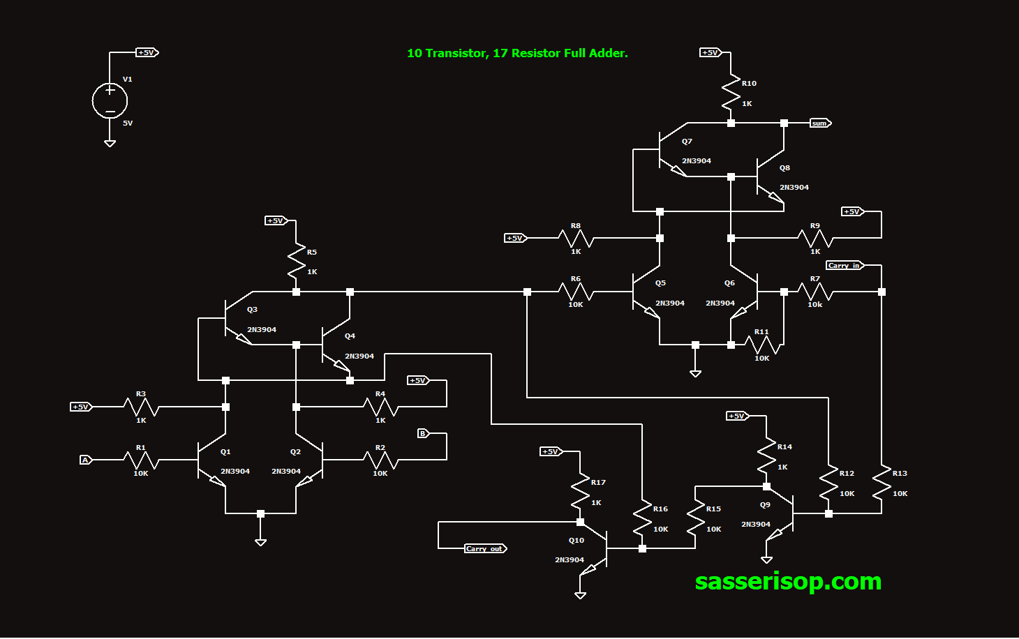
A full adder is a series of logic gates strung together for the purpose of adding two binary numbers together. The goal of my design is to create a robust full adder from BJT transistors and with the minimum number of components, ideally prioritizing minimum transistor count. Fig 1 shows my first design.
Fig 1: A full adder in 10 transistors, 17 resistors
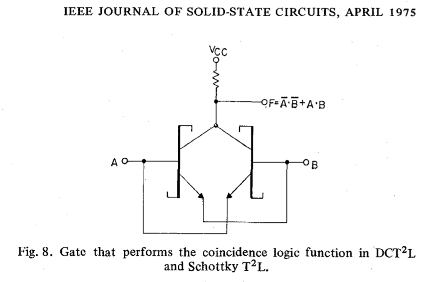
You might notice a pattern, a motif in the design. Part of the reason of the designs small scale is due in part to this two transistor XNOR gate featured in this hackaday post. Two transistors!!! For an XNOR! Crazy. Needless to say I tried shoving this motif everywhere I could.
Fig 2: The forbidden two transistor XNOR gate:
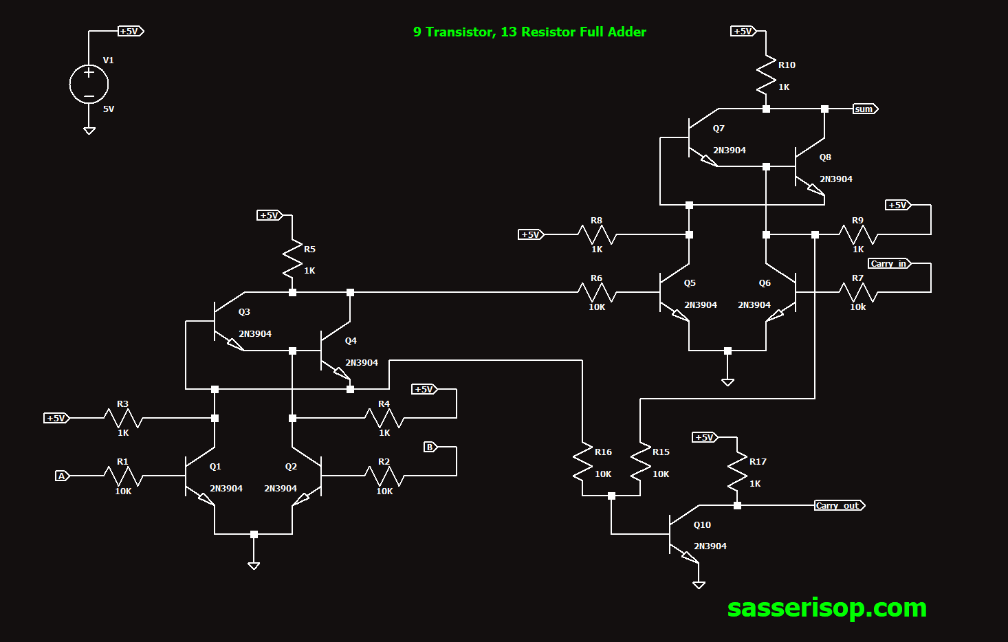
After some late night thinking, I realized a way to remove yet another transistor from the design. I immediately hopped out of bed and started modifying the circuit on the breadboard. To my plesant surprise, the new circuit shown in Fig 3 works.
Fig 3: A full adder in 9 transistors, 13 resistors
But how do these circuits work? Let's jump back to the two transistor XNOR gate. It is the building block of this design. Try this interactive circuit simulation! (Hint: click Run to start the sim.)
Notice how the red output LED turns on if and only if there are an even number of switches switched to the VCC position. This is the definition of XNOR. (You can vary the switches positions by clicking on the diagonal line beside the word INPUT.)
Also notice how I'm kinda cheating by using SPDT switches (single pole, double throw). Look what happens when we try using SPST switches:
The circuit doesn't work! Flipping the switches has no effect on the output. The reason being is that we need a low impedance path to ground, without it there's no way to pull the voltage on the led's anode down, as a result, the led output is stuck on.
We can fix this by adding an input buffer. In this case I use a transistor in a configuration called common-emitter amplifier for each input.
Notice how when the switch is closed, it connects the base of the common-emitter amplifier to VCC, which in turn ties its output to gnd. In essence it's logically inverting the input, this is just a property of this amplifiers topology. In this case what the circuit is really computing is (not A)XNOR(not B). The cool thing is this is logically equivilant to (A)XNOR(B), the two not's cancel out!
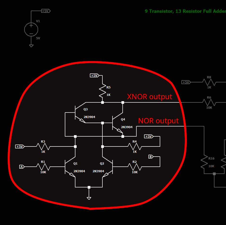
"Okay that's cool but our 2 transistor XNOR gate is now a 4 transistor XNOR gate :(" is what you're probably thinking, but fear not! The reason why I love this topology so much is that it also computes the NOR of it's two inputs for free! I discovered this empirically while messing around. Look at this simulation where I added a green LED:
The green led output is on if and only if all inputs are off. This is the definition of NOR! We can also say the output is off if and only if any of it's inputs are switched on. These two statements are logically equivilent in this context. (For funzies, try coming up with your own logically equivalent statements for the XNOR and NOR gates!)
And with that, we have built the original motif in the full adder circuit. These three circuits are equivalent in function:
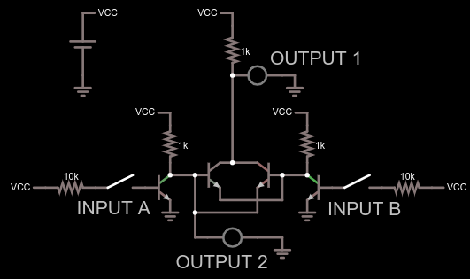
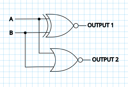
Now let's look at what we need to build a full adder:
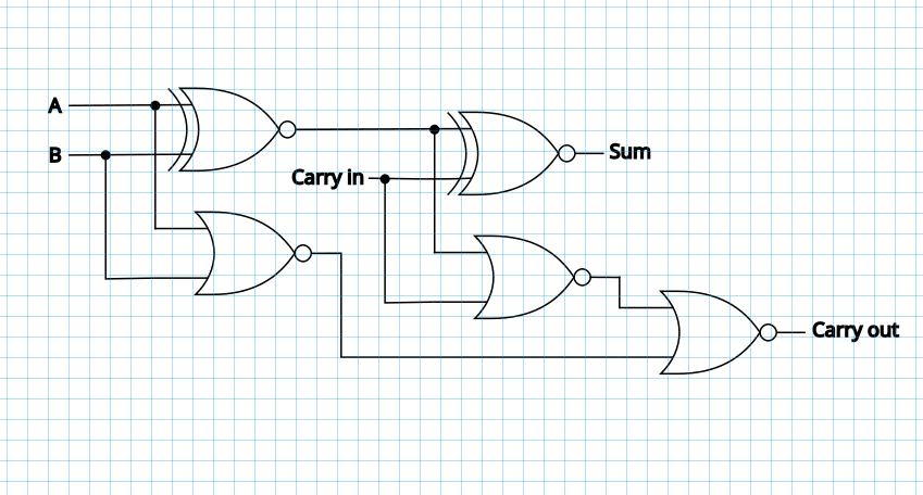
Well, it looks like we can duplicate and daisy chain our design to get 90% of the full adder. All that's left is one more NOR gate for the carry output and that can be done with a single transistor:
Notice the reappearance of the common-emitter amplifier here. It's being used to logically invert the average voltage of A and B. This is NOR!
Now all we have to do is put it all together. If you do so, what you end up with is the circuit from Fig 3. Yay! We have built a 9 transistor full adder. Now you might be asking: "Okay that's cool and all but how the hell does this thing add?" Peep this. (This one might lag your PC! Tip: pan around using ALT+left click):
What you are looking at is a 4-bit full adder. It adds two 4 bit numbers and spits out the result on the right. The circuit is initialized with B=0111, A=1011 and you can see the resulting sum is 10010. In decimal this translates to 11+7=18. So the math works! Look how it's just a daisy chained version of the circuit we designed earlier, it might seem bizarre how some arbitrary collection of logic gates can add. Basically what's going on is each full adder is doing long addition but only for one bit position and it's doing it in binary instead of the base-10 system which humans normally do arithmitic in. By chaining n full adders together we can sum numbers that are n binary digits (bits) wide. Each full adder looks if there was any 1 carried from the digit before as well as looking at the A and B inputs. From this it determines the sum and if it needs to carry a 1 for the next digit in front. It's really just like how we learned to add in elementary school but now we're letting the silicon do all the work for us!
And with that we are finished. I know that I glossed over some stuff like how transistors work and how binary works and how to do long addition in binary and why we're even adding numbers using a binary system when we could use other systems for representing numbers electrically. Perhaps I will add additional pages in the future to supplement this but there are already great resources out there that should calm all your qualms for knowledge. In the future I would like to build a full scale functional computer with just resistors and transistors alone. I think that would be pretty cool. Stay tuned!
Feel free to use my design and illustrations, just credit me if you decide to use it, I am licensing it under CC BY 3.0. Huge thanks to Paul and Iain and all the contributers for the circuitjs web app which is licensed under GNU GPLv2. I also used LTspice, and Inkscape to make the assets and I wrote the html for this page in XFCE's text editor mousepad. Last changes made: Aug 27, 2023